
One of the more exciting pieces we have been working on lately is the Intel IPU. While we wait for the new Intel Mount Evans IPU ASIC DPU, we were able to get some time with the Big Spring Canyon FPGA DPU recently in an Intel (ex-Altera) lab in Santa Clara, California. While I was there, we recorded a demo and hopefully, this helps more of our readers have that “ah ha!” moment where the concept clicks.
As a quick disclosure, I did have to travel to California from Austin so this was a sponsored article/ video. As always, I was able to pick the topic, the STH team retained editorial independence, and Intel did not get to review this before going live, but we want to let everyone know what is going on.
We also were able to do a video of this one, which is our first recorded in three different locations that you can find here:
Many will find that to be a more exciting version since we have a lot of screens where we can explain scrolling text for this one. As always though, we suggest opening the video in its own window, tab, or app for the best viewing experience.
Intel IPU Lines
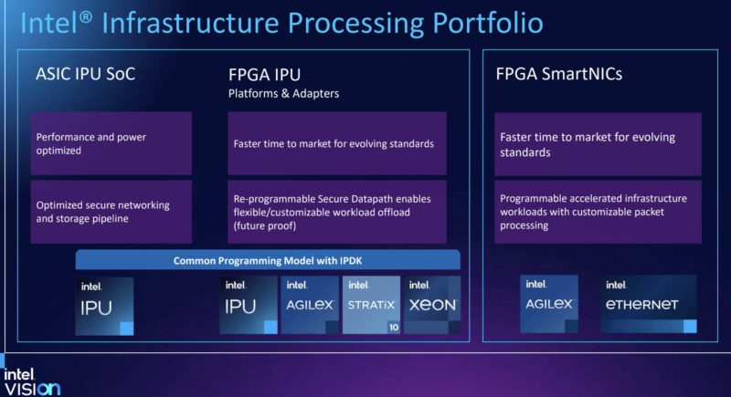
Although we have covered this a lot on STH, Intel essentially has two major IPU lines at the moment. IPU is the Intel-specific term for its “Infrastructure Processing Units” that others in the industry generally call DPUs. It should also not be confused with the Graphcore IPUs that are that company’s current AI processors, even though you could, in theory, have Graphcore IPUs for AI, and Intel IPUs for networking, in the same system. Intel’s two major IPU lines are its ASIC-based solutions that are coming soon, and its FPGA-based solutions like we are looking at here.
An example of the ASIC version is the upcoming Intel Mount Evans IPU/ DPU that Google and Intel co-announced. This is an ASIC with an Arm-based processor.
The FPGA-based IPUs look like they will continue to utilize FPGAs alongside x86 processors and that is what we are looking at in this article.
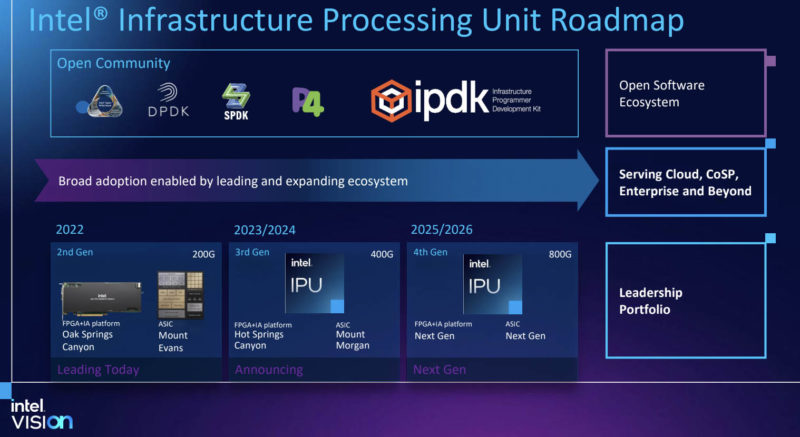
Intel has shown roadmap support up to the 2025/2026 800G generation for both solutions. As time goes on, expect refinements and more performance compared to what we are demonstrating here.
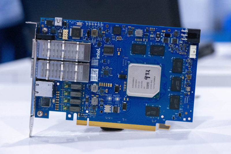
With that, let us get to the card we are looking at, Big Spring Canyon.
Intel Big Spring Canyon IPU
The actual Intel IPU that we used was in a rack of 2U Supermicro Ultra servers. We are just going to note quickly that we did this in a lab environment, so cabling was not what one may call “beautiful”. This was a demo that was quickly set up in a lab.
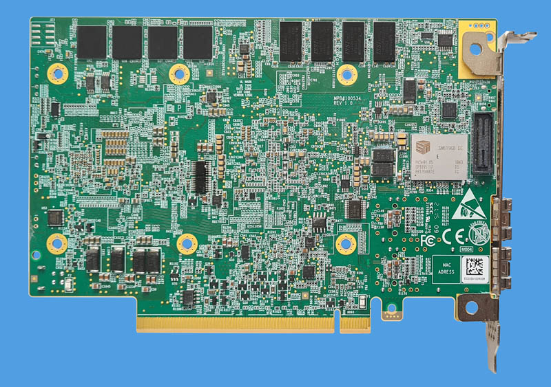
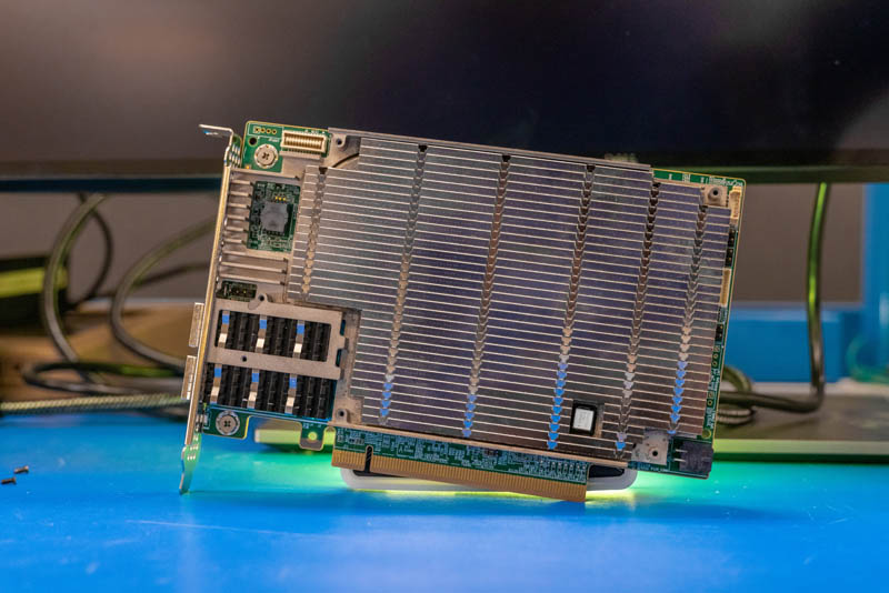
We also had a sacrificial card that we used to disassemble. Part of the intrigue with this card is that onboard is both an Intel Stratix 10 FPGA as well as an Intel Xeon D-1612.
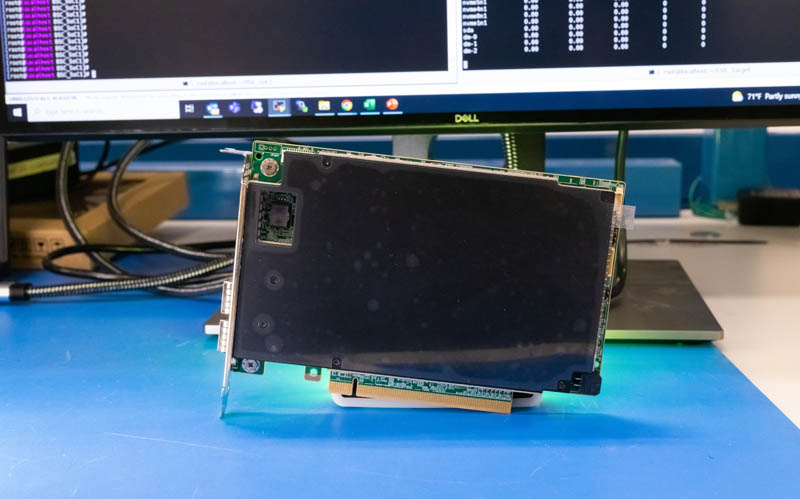
Here is a card with the heatsink assembly removed. We can see the Stratix in the middle with a Xeon D-1612 on the right-hand side. Each has its own memory and there is also local storage since the Xeon D is running its own OS.
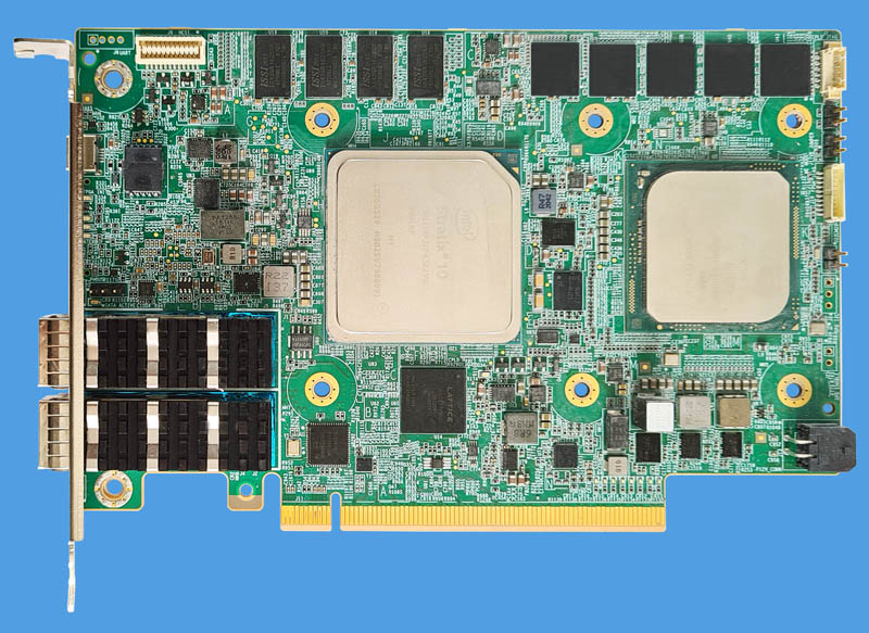
The Stratix 10 FPGA has the PCIe and Ethernet IP hardened. It then has features like a packet processor, virtio, NVMeoF and more that are running on the FPGA. The Xeon D connects through the FPGA on this card.
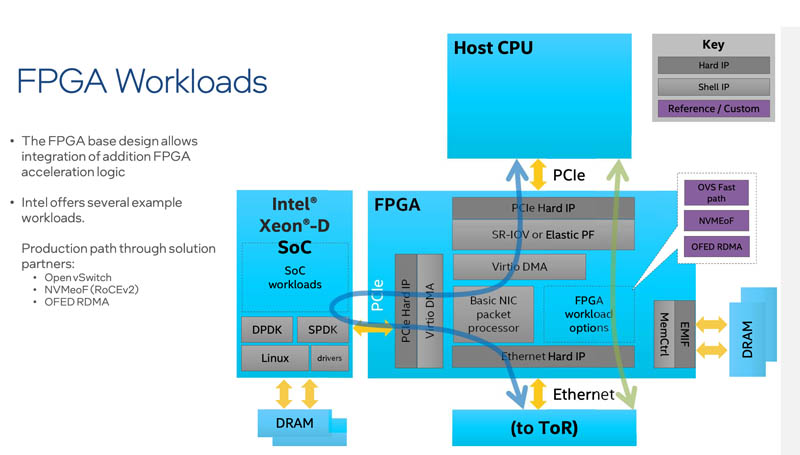
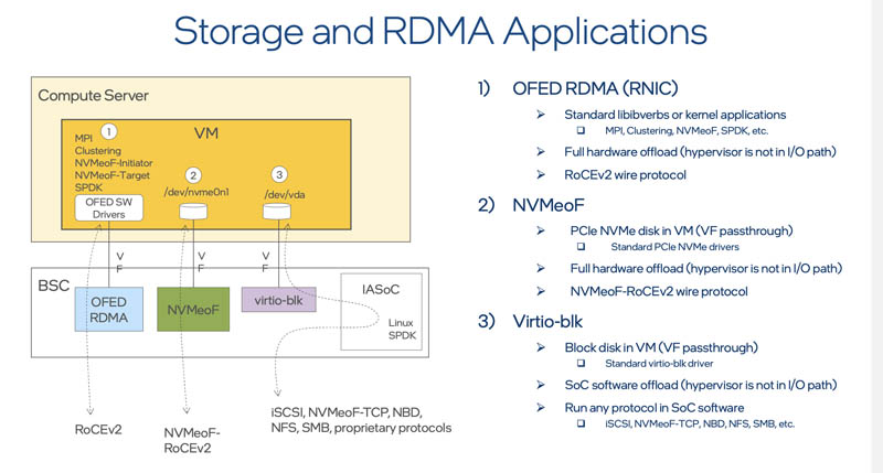
We are going to be showing a NVMeoF demo where the BSC IPU is handling RDMA NVMeoF for the system and is managed by the Xeon D SoC. One of the key benefits here is that the entire stack is offloaded so the host server thinks that it is transacting with a normal NVMe device while the IPU is actually going over the network to remote storage. It is simply emulating a NVMe block device to the system.
Here is the back of the card also without the heat spreader.
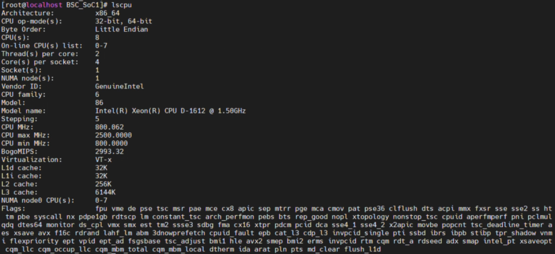
Logging into the Xeon D-1612, we can see a 16GB of memory system with four cores and 8 threads. There are also connections to the storage as well as the FPGA.
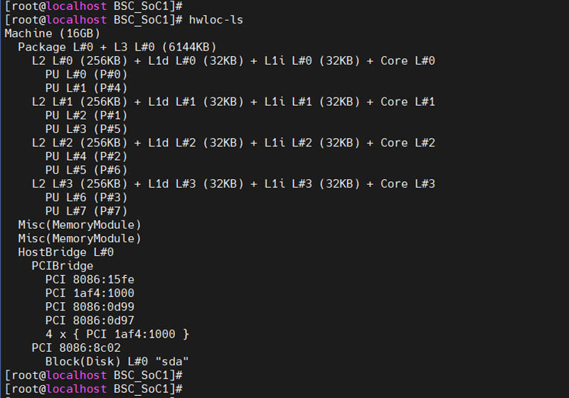
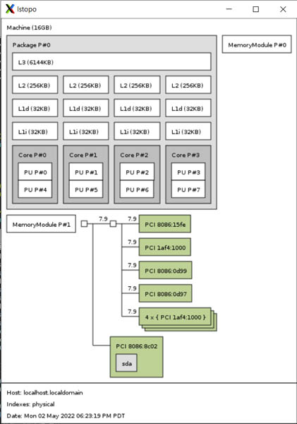
Here is the topology of the IPU as viewed from the Xeon D SoC:
Here is the lscpu output from the Xeon D.
Here is another glamour shot of the card with the top black shroud removed.
Next, let us get into actually using the IPU.


At 22W for the Xeon D-1612 this seems quite a bit more power hungry than the ARM equivalents, any thoughts on that?
Also as this CPU doesn’t support PCIe3.0 it would be interesting to read what the capacity limits are for this DPU, from the face of it it looks like a more power hungry, less performance solution.
Also there’s a likely error in the article stating it has 4 cores 16 threads which should be 8 threads
Has Intel commented on their strategy for encouraging development for the FPGAs?
They are undoubtedly more versatile; but more costly and power hungry than fixed-function equivalents; and writing FPGA implementations, especially good ones, is not baby’s first software project; so this offering seems like it could end up being squeezed between hyperscalers who just revise their fixed-function chips periodically, as events warrant, because they operate so many that the savings cover the engineering costs; while smaller customers will find the flexibility of FPGAs mostly theoretical unless they have access to someone else’s development expertise.
Is Intel the one planning on building and offering a variety of accellerated functions? Are they going to offer a basic library and some sort of 3rd party development program open to very-fabless semicoductor designers who will sell their features and capabilities? A more tightly curated 3rd party program focusing on partnerships with specific interested parties(like hypervisor vendors and makers of various network-disaggregated storage and other peripherals; or high speed packet inspection and modification?
It’s certainly a neat looking part; but the FPGA just seems like something that really needs a software strategy behind it in order to realize its potential.
Sponsored or not, this is a very interesting article! Thanks Patrick!
I don’t know. Sometimes I think STH sponsored is better than other sites non-spons. I’d say this is the best content Intel has for it’s IPUs anywhere that’s public. Maybe it’s also because we’ve seen STH use other tech too. It’s rare to get content like this. I can imagine how the convo on the article went.
Intel: “Hey we need you to have an article like Moore Insights.”
STH: “No. I want lstopo.”
@Kiko Lee: At a bare minimum STH sponsored is usually quite detailed; rather than just a thin press release regurgitation, which is always dreadfully disappointing.
At a lot of sites ‘sponsored’ basically means ‘you’d learn exactly as much just by checking PRNewswire’; rather than ‘we poke around as much as possible and add commentary on capabilities and market position and the like; even if we don’t have the opportunity to really get our hand dirty and do some aggressive benchmarking and such’.
That’s a massive virtue right there.
Patrick, thanks a lot for detailed article about Intel IPU!